Solid State Zero Current
Switching DC Switch for DC Power Systems
Wajiha Shireen
Abstract
In
the design of AC switches or circuit breakers used in AC power distribution
systems, the natural zero crossings of AC currents are used. In DC systems,
when DC currents need to be interrupted due to fault conditions or due to
distribution needs, the arcing current is a major problem. This paper proposes
a DC switch circuit, where the main switch carrying DC load current can be
turned off at zero current. The circuit includes an auxiliary switch, resonant
components, and diodes to aid the zero current switching of the main switch.
The proposed technique has been verified by simulation using PSpice and
experimental results from a hardware prototype.
Index Terms - Distributed Power Systems, Soft Switching
Techniques, DC-DC Converters.
Introduction
The use of electric power shows an increasing trend in all possible avenues of modern civilization. In space applications, equipment used for communication and navigation, control systems, pumps, actuators, precision-timing devices and life-support systems, for example, all require electric power in some form. To keep pace with these high-technology subsystems, intelligent power distribution systems must be developed to switch, protect, and manage the distribution of power. A key element in any power distribution system is the circuit breaker. Circuit breakers have traditionally employed mechanical methods to interrupt excessive currents. While conventional circuit breakers are suitable for most applications, the high-technology subsystems listed above would be better suited to more sophisticated circuit breakers. In the last twenty years, the technology of circuit breakers has dramatically advanced, now including mature devices based on gas-blast (such as SF6) and vacuum interruption.1-3 At the same time, the technology of power electronics devices has evolved rapidly, leading to suggestions of a purely static circuit breaker based on solid-state electronic devices.4-8 Advantages of solid-state breakers include faster fault current interrupting capability, increased reliability, and intelligent power control. Moreover, solid-state breakers can provide automatic or remote resetting. This has generated interest in replacing mechanical circuit breakers with solid-state equivalents.
In the design of AC switch or circuit breakers used in AC power distribution systems, the natural zero crossings of AC currents are used. In contrast to AC systems, the fundamental problem of breaker operation in DC systems is the absence of current zeros. DC transmission circuits usually have large inductances in the form of smoothing reactors and long transmission lines. Therefore, one of the ways that direct current can be brought to zero is by applying a counter voltage in excess of the driving voltage. A typical DC breaker attempts to insert this counter voltage or breaker voltage in one manner or another. While bringing the direct current to zero, the breaker has to absorb significant amounts of energy.
In this paper, a solid-state DC switch circuit is proposed,
where the current through the main switch is brought to zero by providing an
alternate path for the DC load current with the help of an auxiliary switch and
resonant components. Advantages of the proposed solid-state DC switch/breaker
circuit include reset ability, increased reliability, intelligent control and automatic
and remote resetting.
The proposed DC Switch Circuit
Figure 1 shows the DC switch circuit. The circuit consists
of the main switch T1, the auxiliary switch T2, resonant
components Lr and Cr along with
diodes D1, D2, and D3. The main switch T1 is in the main current
path connecting the source Vs to the load. The load is considered to
be an RL load. Under normal operating conditions, switch T1 is ON
carrying the load current Im , and the auxiliary switch T2 remains
OFF.

Figure 1: The proposed DC Switch Circuit
The operation of the DC switch circuit can be divided into six modes. The circuit configurations of each mode are shown in Figure 2. The proposed circuit was simulated using PSpice, and the operating principle can be explained by the aid of the simulated current and voltage waveforms shown in Figure 3.
Initially, the DC voltage Vs is supplying energy to the load through the primary switch (T1). The auxiliary switch T2 is activated, and the following modes of operation take place.
Mode 1: At t = t0, the resonant switch (T2) is turned ON. The primary switch T1 continues to conduct the load current Im , and a resonant current pulse flows through the LC branch, charging the capacitor Cr. The capacitor current and voltage are given by,
![]() , (1)
, (1)
![]() , (2)
, (2)
where Vo is the initial voltage
across the capacitor, and ![]() is the resonant
frequency given by
is the resonant
frequency given by ![]() . This mode ends at
. This mode ends at ![]() , when the capacitor current ic(t)
goes to zero as shown in Figure 3 and T2 is turned OFF with zero
capacitor current. From equation (2),
the peak capacitor voltage at
, when the capacitor current ic(t)
goes to zero as shown in Figure 3 and T2 is turned OFF with zero
capacitor current. From equation (2),
the peak capacitor voltage at ![]() is given by,
is given by,
![]() . (3)
. (3)
Mode 2: The capacitor current reverses its direction and flows through diode D1 such that
![]() . (4)
. (4)
The current through T1 decreases as ic(t) increases, and when ic(t) = Im at t = t2 , T1 is turned OFF with zero current. The capacitor voltage for this mode is
![]() . (5)
. (5)
Mode 3: The voltage and current equations for this mode are the same as for Mode 2. The excess current ic(t) - Im flows back to the source through diode D2. This mode ends when ic(t) again becomes equal to Im at t = t3.
Mode 4: The capacitor continues to discharge in a constant current mode. The capacitor current and voltage equation are as follows:
![]() , (6)
, (6)
and ![]() . (7)
. (7)
where Vc2 is the capacitor voltage at the end of Mode 3. This mode ends when vc(t)=0 at t = t4 and the load current freewheels through D3 and D1.
Mode 5: The capacitor voltage and
current in this freewheeling mode are given by, ![]() , (8)
, (8)
![]() (9)
(9)
This mode ends when the capacitor current falls to zero at t = t5.
Mode 6: Diode D3 will come into conduction as soon as the capacitor current goes to zero at t = t5. At the end of this mode, i.e. at t = t6, the capacitor will be charged to a positive Vo .
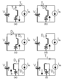
Figure 2 : Operating modes of the proposed circuit. (a) Mode1 (b)Mode 2 (c) Mode 3 (d) Mode 4 (e) Mode 5 (f) Mode 6
|
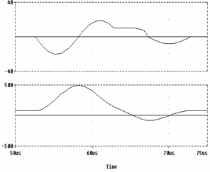
Vo t2 t6 t5 t4 t3 t1 t0 2Vs-Vo Vc2 M6 M5 M4 M3 M2 M1 Capacitor
voltage Capacitor
current Figure 3 Simulated waveforms of the proposed circuit.(Vs=100V, Im=5A) |
Experimental Results
Figure 4 shows the preliminary experimental result of the proposed DC
circuit breaker. The circuit in Figure 1 was implemented in the laboratory. Vs was set to 50 V for the experiment, and the
load was selected to get Im equal to 0.5A.
In addition to the DC switch circuit described above, the implementation
involved the gate-driver circuit and the control circuit. The control circuit
monitors and advances the switch circuit through its modes. The gate-driver
circuit is the interface between the control circuit and the power circuit that
provides isolation and provides enough power to the control signals to operate
the power semiconductor devices (T1 and T2). The control
circuit was implemented, using three monostable multivibrators which provided a set delay time and advance
the circuit to the next mode. The lower trace in Figure 4 shows the current
through the main switch T1. The upper trace in Figure 4 shows the
control signal for T1. It can be seen that the current through the
main switch T1 is brought down to zero before the gate-command
signal turns T1 OFF. This facilitates DC current interruption
without causing any arcs. Figure 5 shows the current through the resonant
capacitor (lower trace) and the voltage across the resonant capacitor (upper
trace). It can be seen that the experimental results shown in Figure 5 match
the simulation results shown in Figure 3.
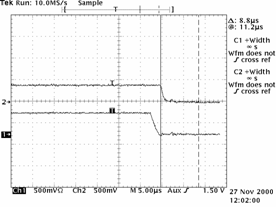 |
Figure 4
Upper trace – Gate control signal for T1
Lower trace – Current through T1
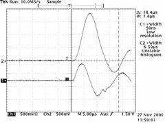 |
Figure 5 Upper trace – Voltage across the resonant capacitor (25V per division)
Lower trace – Current through the resonant
capacitor (0.5A per division)
Conclusion
A solid state DC circuit breaker using soft switching technique is
proposed and implemented using a laboratory prototype. The proposed circuit
breaker facilitates interruption of DC currents by providing an alternate path
for the main current and thereby allows zero current switching (no arcs).
References
[1] T.M. Jahns, R.W.A.A. De Doncker, J.W.A. Wilson, V.A.K. Temple, and D.L. Watrous, “ Circuit Utilization Characteristics of MOS-Controlled Thyristors,” IEEE Transactions on Industry Applications, vol. 27, no. 3, pp. 589-597, May/June 1991.
[2] R.W.A.A. De Doncker, T.M. Jahns, A.V. Radun, D.L. Watrous, and V.A.K. Temple, “Characteristics of MOS-Controlled Thyristors under Zero Voltage Soft-Switching Conditions,” IEEE Transactions Industry Applications, vol. 28, no. 2, pp. 387-394, March/April 1992.
[3] E. Yang, V.
[4] L. Malesani, et. al., “A synchronized resonant DC-link converter for soft switched PWM”, IEEE Industry Applications Society Conference Records, 1989, pp.1037-1044.
[5] Ned Mohan et. al., “Parallel resonant DC link circuit - A novel zero switching loss topology with minimum voltage stresses”, IEEE Power Electronics Specialists Conference Records, 1989, pp.1006-1012.
[6] Ned Mohan et. al., “Zero voltage switching PWM inverter for high frequency DC-AC power conversion”, IEEE Industry Applications Society Conference Records, 1990, pp.1215-1221.
[7] B. K. Bose et. al., “An improved resonant DC-link inverter for induction motor drives”, IEEE Industry Applications Society Conference Records, 1988, pp.742-748.
[8] B. K. Bose et. al., “High frequency quasi-resonant DC voltage notching inverter for ac motor drives”, IEEE Industry Applications Society Conference Records, 1990, pp.1202- 1207.